
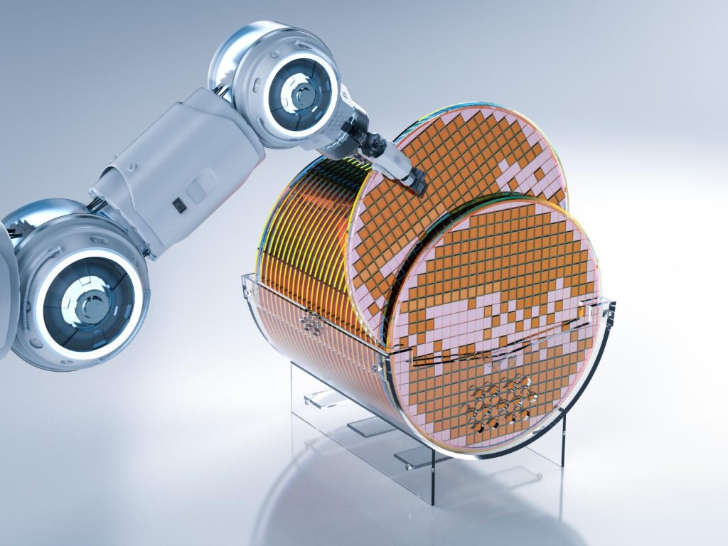
The semiconductor industry is on the cusp of a new era as Taiwan Semiconductor Manufacturing Company (TSMC) gears up to commence mass production of its groundbreaking 2 nm Gate-All-Around (GAA) node in late 2025. This milestone represents the culmination of years of research, development, and capital investment aimed at sustaining Moore’s Law and delivering unprecedented gains in performance, power efficiency, and transistor density. The 2 nm node will underpin the next generation of high-performance computing, mobile devices, and specialized accelerators for artificial intelligence workloads. As TSMC moves from risk production through pilot runs to high-volume manufacturing, the company’s manufacturing ecosystem—from equipment suppliers to material innovators—has been rigorously stress-tested. This transition promises to reshape chip design paradigms, bringing radical advantages to system-on-chip integrators and their end users. In the following sections, we examine the evolution of transistor scaling toward 2 nm, delve into the technical breakthroughs of GAA architecture, chart TSMC’s development milestones, explore the formidable manufacturing challenges, assess the broader industry implications, and glimpse the research frontiers that lie beyond the 2 nm node.
Evolution of Semiconductor Node Scaling Toward 2 nm
The march from 90 nm to 2 nm has been characterized by relentless innovation across lithography, materials science, and device architecture. Early nodes relied on planar transistors etched with optical lithography, but as feature sizes shrank below 20 nm, leakage currents and variability plagued device performance. In response, the industry adopted FinFET transistors at the 22 nm node to confine current more effectively, and successive refinements at 16 nm and 7 nm improved fin height and width for better electrostatic control. However, today’s architectures demand even tighter gate control and reduced short-channel effects, driving the shift to Gate-All-Around devices, where the transistor channel is wrapped by multiple nanosheets or nanowires. Achieving the transition to 2 nm has required multiple disruptive advances: extreme ultraviolet (EUV) lithography to pattern sub-30 nm features in high-volume, new high-k metal gate stacks to maintain threshold voltages, and novel spacer and etch processes to define ultrathin channels. Materials innovation—such as cobalt contacts, cobalt-tungsten liners, and ruthenium interconnects—has been instrumental in controlling resistance and electromigration at such scales. Taken together, this evolution underscores a departure from mere geometric scaling toward holistic co-optimization of device physics, materials, and process integration to sustain performance gains.
Gate-All-Around Transistor Architecture and Its Advantages
At the heart of TSMC’s 2 nm node lies the Gate-All-Around transistor, leveraging stacked nanosheets as the active channel material. Unlike FinFETs, where only three sides of the channel are controlled by the gate, GAA nanoribbon or nanosheet transistors fully encircle the channel, providing superior electrostatic control that dramatically reduces off-state leakage and variability. This architecture enables aggressive threshold voltage modulation, supporting lower supply voltages while maintaining high drive currents. The stacked nanosheet design further permits dynamic channel width adjustment by altering the number or thickness of sheets, offering flexibility for performance- or power-optimized libraries on a single die. In practical terms, GAA transistors deliver a double-digit percentage improvement in energy per operation and a commensurate boost in switching speed compared to FinFET counterparts at similar nodes. Additionally, the planar top view of nanosheets simplifies gate patterning and reduces device footprint, enhancing overall transistor density. These combined benefits translate to the potential for over one trillion transistors on a single large-format wafer, unlocking new possibilities for integrated AI accelerators, heterogeneous chiplet assemblies, and ultra-efficient microcontrollers powering the IoT.
TSMC’s 2 nm Development Milestones and Timeline
TSMC embarked on its 2 nm roadmap in the early 2020s, leveraging its extensive experience with 5 nm and 3 nm tri-gate FinFET platforms. Initial research focused on material compatibility, with pilot lines exploring nanosheet formation via selective epitaxial growth and sacrificial layer removal processes. By mid-2022, TSMC reported successful fabrication of sub-3 nm GAA prototypes at its Fab 14 in Taiwan, demonstrating robust subthreshold slope and drive-current characteristics in laboratory conditions. In 2023, the company initiated risk production for its 2 nm trial wafers, integrating EUV for multiple patterning steps and refining gate work functions through atomic layer deposition. Late-2024 saw the commencement of early pilot production runs aimed at yield ramp optimization, as TSMC worked to reduce defect densities through advanced inspection and metrology tools. Parallel collaborations with key equipment suppliers—such as ASML for high-NA EUV systems and Applied Materials for selective CVD chambers—ensured that tool readiness matched process maturity. With yields approaching commercial viability in early 2025, TSMC now plans to open its Fab 18 for mass production, targeting a volume capacity of several hundred thousand wafers per month by Q4 2025. This aggressive yet calibrated timeline positions TSMC to meet customer demand for flagship SoCs and datacenter GPUs requiring the most advanced transistor performance.
Challenges in Manufacturing at 2 nm Scale
Manufacturing at the 2 nm scale introduces unprecedented challenges that span materials, equipment, and integration complexity. First, controlling variability in nanosheet dimensions demands atomic-level precision in epitaxial growth and etch uniformity across 300 mm wafers. Small deviations of even a single atomic layer can shift threshold voltages and degrade performance. Second, extreme ultraviolet lithography at high numerical aperture (NA) introduces new overlay and focus control requirements, necessitating sub-2 nm overlay accuracy and advanced pellicle designs to manage mask contamination. Third, as interconnect pitches shrink below 20 nm, maintaining low resistance and robust reliability requires novel materials such as cobalt or ruthenium liners and ultra-thin low-k dielectrics, while ensuring manufacturability at scale. Fourth, thermal budgets tighten, as high temperatures can cause diffusivity-driven profile changes in dopants and metal alloys. Fifth, defect detection and yield learning must operate at nanometer sensitivity, pushing metrology tools to their limits and driving adoption of AI-accelerated inspection algorithms. Finally, cost per wafer escalates significantly, demanding optimized cycle times and high write-week economics to justify the investment. Addressing these challenges has involved co-development agreements between TSMC, equipment vendors, and advanced materials suppliers, culminating in tight process control and continuous learning loops to improve yield.
Implications for Industry and Global Technology Leaders
The arrival of 2 nm GAA technology will reverberate throughout the semiconductor and broader technology ecosystems. Chip designers at companies like Apple, Nvidia, AMD, and Qualcomm will gain access to unprecedented performance-per-watt envelopes, enabling smaller, faster mobile processors and more power-efficient datacenter accelerators. This advancement will also sharpen competitive distinctions: firms that secure early design wins on TSMC’s 2 nm node can define new markets and reinforce customer loyalty. Conversely, foundries still operating on older nodes may face accelerated margin erosion and customer migration. Geopolitical dynamics will intensify, as countries seek to secure advanced packaging capabilities and supply-chain resilience for strategic semiconductor infrastructure. The high capital costs associated with 2 nm fabs—estimated at over $20 billion per facility—will further consolidate the foundry landscape, reinforcing TSMC’s leadership and challenging rivals to pursue niche specializations or alternative materials like monolithic 3D integration. For end users, the proliferation of 2 nm chips will usher in new form factors and use cases: AI-powered wearables, autonomous vehicles with advanced sensor fusion, and cloud services offering quantum-inspired simulations at scale. The economic ripple effects will extend into equipment manufacturing, materials innovation, and workforce development, shaping the next chapter of global technology leadership.
Future Prospects Beyond 2 nm: Research and Roadmap

While the 2 nm GAA node represents a significant inflection point, TSMC and its partners are already charting pathways to sub-2 nm and beyond. Research into stacked gate-all-around nanowire transistors with diameters under 3 nm, as well as monolithic three-dimensional integration, promises further density gains and vertical stacking of logic and memory. Advanced lithography techniques—such as high-NA EUV capable of patterning below 10 nm pitches—and directed self-assembly methods may become mainstream by the latter half of the decade. Alternative channel materials like germanium or III-V compounds are being evaluated for their higher mobility characteristics, while spintronics and ferroelectric transistors offer potential non-volatile logic-in-memory solutions. Novel device architectures that integrate photonic interconnects at the die level could alleviate the performance constraints of copper wires at scale. Simultaneously, the semiconductor industry is exploring new system-level paradigms—such as chiplet-based heterogeneous integration and wafer-scale computing fabrics—that can complement transistor-level scaling. As device reliability, manufacturability, and cost challenges are addressed, the roadmap beyond 2 nm envisions a multi-pronged approach combining incremental materials innovation, architectural breakthroughs, and radical co-design of hardware and software stacks. This long-term vision underscores the enduring importance of collaboration between foundries, equipment suppliers, academic researchers, and system integrators to propel the next revolutions in computing.


Leave a Reply